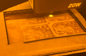
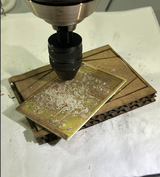
Advances in desktop lasers have made them useful for printed circuit board design. While the process is still being tweaked, I have found that a thin, even layer of varnish protects the PCB during etching. Then you put this into an acetone bath, and the acrylic varnish breaks down, revealing the PCB traces. I am also trying to migrate to Surface Mounted Devices because drilling a lot of holes is tedious. While it’s fun to use the power drill, I’d cut the process time by using SMD alone instead of drilling and punching holes.
Then you lay the components out and assemble it. Granted, my fabrication process typically produces 4 identical boards on the current scale I am working with. The more hardware I duplicate, the better, because you are creating consistency.
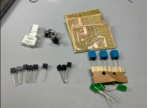
You’re probably wondering why there are different boards. I’ve fabricated up to 10 PCBs so far this month. Most of the circuitry is on monolithic and discrete-logic boards that handle basic functions like generating pulses and switching power.
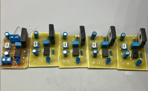
The goal is consistency and process refinement. Though I am very aware that I could send these to a PCB Fabricator and wait 5 business days to receive them. I just find it fun taking two to three days to create something in-house. Plus, I get to use tools and refine my skills. If I needed 10+ or a lot, I would send it to a PCB Fabricator. But for now, making it myself is simple. It’s just time, effort, and money.